
Electronics and Control is an optional area of study in Leaving Certificate Technology at Higher Level. It builds on what you already know about electricity and logic gates from the core. Everything in this option follows one clear systems path: an input stage (such as a switch or sensor) detects a condition, a process stage (transistors, operational amplifiers, logic gates, timers, or counters) decides what to do, and an output stage (lamps, LEDs, buzzers, relays, or d.c. motors) produces the action. You will learn to calculate circuit quantities, select appropriate components, assemble prototypes on breadboards, test and fault-find systematically, and manufacture finished printed circuit boards (PCBs). Under the 2027 Leaving Certificate Assessment Arrangements, the terminal written examination lasts 2½ hours and contributes 50% of your total marks. In Section C, you answer one of the five long option questions. The remaining 50% of the subject is allocated to coursework (100 marks for the design folio and 100 marks for the artefact). The 2027 Higher Level coursework brief requires an electro-mechanical solution powered by a low-voltage electrical supply to support independent living, wellbeing, or social participation in an ageing society. Mastering this option gives you the calculation methods, circuit blocks, and testing procedures needed for Section C and your coursework artefact.
1. Electrical Measurements, Resistor Networks, and Power Calculations
Working with electronic circuits requires measuring fundamental physical quantities using standard SI units and connecting instruments correctly without disturbing the circuit:
- Potential difference (): Measured in volts (V) using a voltmeter connected in parallel across a component. A voltmeter has a very high internal resistance, so it draws negligible current from the circuit.
- Electric current (): Measured in amperes (A) using an ammeter connected in series by breaking the circuit loop. An ammeter has a very low internal resistance, so it barely reduces the current it is measuring. Connecting an ammeter in parallel across a power supply creates a direct short circuit.
- Electrical resistance (): Measured in ohms () using an ohmmeter or multimeter resistance range. The component must be fully isolated from any power source before taking a reading.
- Capacitance (): Measured in farads (F), with microfarads (, ), nanofarads (nF, ), and picofarads (pF, ) used in practical circuits. Measure capacitance using the capacitance range of a digital multimeter or a dedicated LCR meter. Always discharge the capacitor safely before testing.
- Frequency (): Measured in hertz (Hz, cycles per second or ). Measure frequency using the frequency range of a multimeter, or an oscilloscope by measuring the period of one complete cycle ( in seconds) and applying .
Quick Meter Connection Summary
- Voltmeter: connected in parallel, internal resistance very high.
- Ammeter: connected in series, internal resistance very low.
- Ohmmeter: power off, component isolated.
- Capacitance: multimeter capacitance range or LCR meter, capacitor discharged first.
- Frequency: multimeter Hz setting or oscilloscope using .
Resistors in Series and Parallel
- Resistors in series: . The same current flows through both, and the total resistance is the sum of the individual values.
- Resistors in parallel: , which can also be calculated as . The total equivalent resistance is always smaller than the smallest individual branch. For example, two resistors in parallel give an equivalent resistance of .
Indirect Measurement of Power
Power (), measured in watts (W), is the rate of electrical energy transfer. In Technology examinations, power is determined indirectly by measuring voltage and current separately and applying:
Combining this with Ohm's law () allows power dissipation to be calculated when only two of the three variables are known:
Every physical resistor has a safe power rating (typically 0.25 W or 0.5 W in school projects). If a resistor carries (), its power dissipation is . A standard 0.25 W resistor would burn out under these conditions, so a component rated for at least 0.5 W must be selected.
2. Circuit Components, Circuit Symbols, and Potential Dividers
Circuit diagrams communicate designs using standardised schematic symbols. In an exam answer or design folio, always draw the positive supply rail (+V) along the top and the zero-volt rail (0 V) along the bottom, and label every component with its type and value.
Essential Circuit Symbols to Recognise and Draw
- D.C. Power Supply / Cell: Long line represents the positive terminal, short thick line represents negative. A battery shows multiple connected cells.
- Fixed Resistor: A plain rectangle. Variable resistor / potentiometer: A rectangle with an arrow across or pointing to it.
- Capacitors: Two parallel plates for non-polarised capacitors; an electrolytic capacitor shows a curved negative plate and an indicated positive terminal.
- Inductor (coil): A coil of wire, drawn as a series of loops (or a solid rectangle on some schematics). It stores energy in a magnetic field and opposes any sudden change in current, making it useful for smoothing or filtering signals. Relay coils and motor windings are inductors, which is why switching them off generates an inductive voltage spike.
- Diodes and LEDs: A triangle pointing against a vertical cathode bar. An LED adds two small arrows pointing outward to indicate light emission.
- Transistors (NPN): A circle containing a base bar, collector lead, and an emitter lead with an arrow pointing outward.
- Output Transducers: A circle with 'M' for a d.c. motor, a speaker symbol, a buzzer symbol, or a relay coil rectangle linked by a dashed line to switch contacts.
Potential Dividers as Voltage Controls
A potential divider divides a supply voltage across two series resistors in direct proportion to their resistance values:
Here is connected between the positive rail and the output junction, while is connected between the junction and 0 V. If is replaced by an analogue sensor (such as an LDR or thermistor), changing environmental conditions cause to rise or fall, providing an adjustable signal to drive a transistor switch or op-amp.
Transistor Switching and Darlington Pairs
An NPN bipolar junction transistor acts as a current-controlled electronic switch. A small base current () switches on and controls a much larger collector current (). The transistor begins conducting only when the base-emitter voltage reaches approximately 0.6 V to 0.7 V. Below this threshold, the transistor remains switched off.
When a single transistor cannot provide enough current gain (), two transistors are connected as a Darlington pair. The collector terminals are connected together, and the emitter of the first transistor feeds the base of the second. The total current gain is the product of the two individual gains (). Because there are two base-emitter junctions in series, a Darlington pair requires a base-emitter switching voltage of approximately 1.2 V to 1.4 V to turn on fully.
3. Analogue Sensors and Signal Conditioning
Sensors are input transducers that monitor physical conditions and convert them into electrical signals. In Leaving Certificate Technology, resistance-based sensors are placed inside a potential divider so that changes in physical conditions produce a changing voltage signal.
Light Sensing
- Photoresistor (Light-Dependent Resistor / LDR): Made from cadmium sulphide. Its resistance decreases as light intensity increases (from several megohms in pitch darkness down to a few hundred ohms in bright sunlight).
- Photovoltaic Cell (Solar Cell): Directly generates an electric potential from light energy without requiring an external bias voltage.
- Photodiode: A semiconductor junction operated in reverse bias. Incoming light increases reverse leakage current. Photodiodes respond within microseconds, making them suitable for fast optical pulse counting and beam-break triggers.
- Phototransistor: Incoming light acts directly as the base current, which is amplified into a larger collector-emitter current. It produces higher output current than a photodiode, though with a slightly slower switching speed.
Temperature, Sound, Moisture, and Motion Sensing
- NTC Thermistor: Negative Temperature Coefficient sensor whose resistance drops as temperature rises. When placed at the bottom () of a potential divider, heating the thermistor lowers .
- Microphone: Converts sound waves into an alternating voltage of a few millivolts. Because this signal is weak, it requires an operational amplifier pre-amplifier stage before it can trigger switching circuits.
- Moisture Sensor: Consists of two open conductive tracks separated by a small gap. Water contains ions that bridge the tracks, dropping the electrical resistance from infinity to several kilohms.
- Motion Sensors: Include optical beam-break pairs (an infrared LED paired with a phototransistor or photodiode), physical microswitches used as mechanical limit sensors, and passive infrared (PIR) modules that detect moving heat sources across optical zones.
4. Power Supplies, Relays, and Coursework Safety
Selecting an appropriate power supply involves matching the operating voltage, current capacity, and portability requirements of your system:
- Mains Electricity (230 V a.c., 50 Hz): High voltage and hazardous. Mains supplies are used for stationary, high-power equipment. A bench power supply converts mains a.c. into low-voltage d.c. using a step-down transformer, a diode bridge rectifier, electrolytic smoothing capacitors, and a voltage regulator IC (such as a 7805 for a steady +5 V output).
- Batteries (Low-Voltage d.c.): Portable, self-contained, and safe. Primary cells (alkaline) are disposable, whereas secondary cells (NiMH, Li-ion) are rechargeable. Battery capacity is measured in milliampere-hours (mAh). The estimated run time is calculated as .
Relays and Electrical Isolation
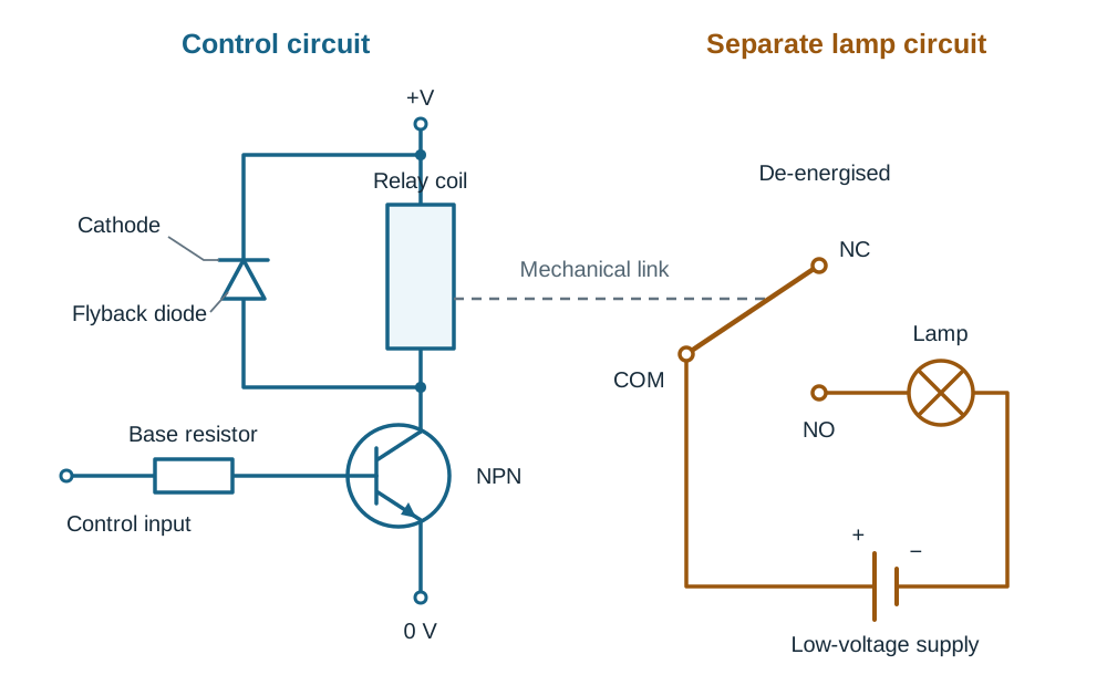
A relay is an electrically operated mechanical switch. Passing current through its internal coil creates an electromagnet that moves an iron armature, opening or closing switch contacts:
- Normally Open (NO): Contacts remain open when the coil is off, and close when the coil is energised.
- Normally Closed (NC): Contacts remain closed when the coil is off, and open when the coil is energised.
- Single-Pole Double-Throw (SPDT / Changeover): Contains both NO and NC terminals connected to a shared common terminal.
A relay provides complete electrical isolation between the low-voltage control circuit (such as a 5 V logic gate or transistor) and the output circuit, which may operate at a different voltage or carry a large direct or alternating current. Because a relay coil typically draws 30 mA to 80 mA, it cannot be driven directly from a logic gate; a transistor driver is required. Furthermore, a reverse-biased flyback diode must always be placed across the coil to clamp inductive turn-off spikes.
Coursework Safety Requirements (2027 Brief)
The SEC instructions to candidates specify that where an electrical supply is used to operate the project artefact, it should be of low voltage output. In school workshops, this means using batteries or a commercial low-voltage bench/plug-top power supply (typically 5 V, 6 V, 9 V, or 12 V)—never candidate-wired mains circuitry. Artefacts must have accessible operating features, incorporate clear operating instructions, and fit within a 500 mm maximum dimension.
5. D.C. Motors: Operation, Back EMF, Efficiency Testing, and Reversing Circuits
A permanent-magnet direct-current (d.c.) motor converts electrical energy into continuous mechanical rotary motion. When direct current passes through the armature coil inside a magnetic field, the coil experiences opposing electromagnetic forces (), producing torque. A split-ring commutator and carbon brushes reverse the current direction through the armature every half-rotation to maintain movement in a single direction.
Rotational Back EMF ()
As the armature spins through the magnetic field, it acts simultaneously as an electric generator. According to Lenz's law, this rotation induces a counter-voltage that directly opposes the applied supply voltage. This induced voltage is the rotational back EMF (), and its value is directly proportional to armature speed.
The net voltage available across the armature resistance () determines the current draw:
| Motor State | Armature Speed | Rotational Back EMF () | Current Draw () |
|---|---|---|---|
| Stalled / Start-up | 0 rpm | 0 V (no generator action) | Maximum stall surge (). Risk of rapid overheating. |
| Running Freely | Maximum rpm | High (e.g. 10.8 V on a 12 V motor) | Minimal idle current (). |
| Under Mechanical Load | Slowed rpm | Decreases (e.g. drops to 8.0 V) | Increases automatically () to deliver higher torque. |
For example, in a 12 V motor with an armature resistance of , the stalled current is . When running freely with , the current drops to .
Experimental Procedure: Measuring D.C. Motor Efficiency
To measure the efficiency of a d.c. motor experimentally:
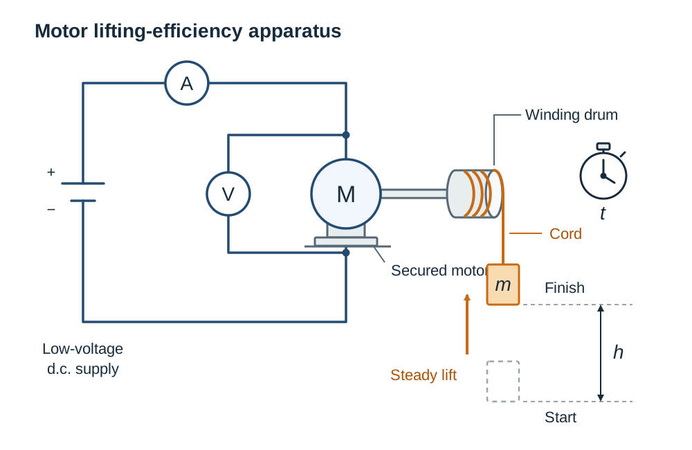
- Secure the motor to a test bench and mount a small pulley or winding drum of known diameter onto the shaft.
- Attach a cord carrying a known test mass ( in kg) and measure the vertical lifting height ( in metres).
- Connect a voltmeter in parallel across the motor terminals and an ammeter in series in the positive supply lead.
- Switch on the supply and, once the mass is rising at a steady speed, record the operating voltage () and current (). Readings must be taken while running, because the start-up surge does not represent steady operation.
- Time the lift using a stopwatch ( in seconds). Repeat three times and calculate the average time to minimise timing error.
- Calculate electrical power input: .
- Calculate useful mechanical power output: (using ).
- Calculate efficiency: .
Energy losses occur due to electrical resistance in the copper windings ( heating), bearing friction, brush-commutator contact resistance, and external friction in the pulley and cord.
Motor Reversing Circuits
Reversing a permanent-magnet d.c. motor requires swapping the polarity of the voltage applied to its terminals:
- DPDT Switch: A Double-Pole Double-Throw switch connected in an X-pattern cross-wiring configuration swaps the positive and negative connections to the motor terminals when thrown.
- Relays: Two SPDT relays (or one DPDT relay) controlled by electronic signals swap supply polarity automatically, isolating sensitive logic from motor current.
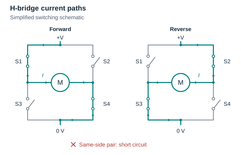
- H-Bridge: An arrangement of four transistor switches around a central motor. Activating diagonal pairs drives the motor forward; activating the opposite diagonal pair drives it in reverse. Switching both transistors on the same vertical branch must be prevented, as it creates a direct short circuit across the power supply rails.
6. Timing Circuits, Astables, and RC Time Constants
Timing and oscillator circuits in Leaving Certificate Technology are built around the 555 timer integrated circuit. Understanding these circuits begins with the charging behavior of a resistor and capacitor.
The RC Time Constant
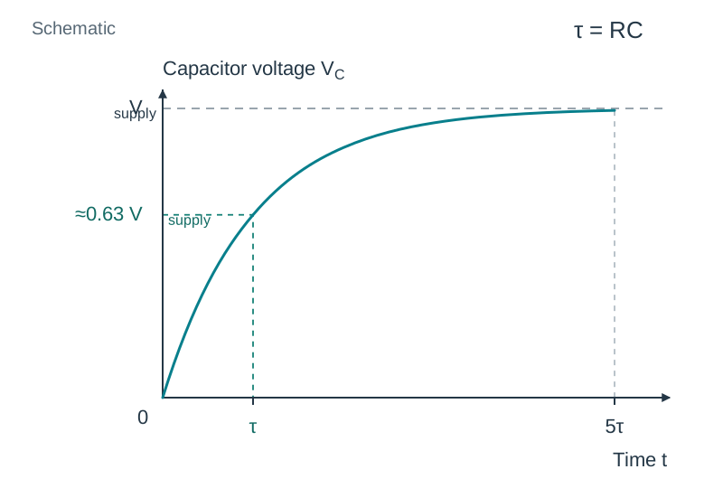
When a capacitor () charges through a resistor () from a d.c. voltage supply, the rate of voltage rise is determined by the RC time constant ():
When is in ohms and is in farads, is in seconds. In one time constant (1), the capacitor charges to approximately 63% of the supply voltage. It is considered fully charged after 5 time constants (). Increasing either or increases charging time, which lengthens time delays and clock pulse periods.
Essential 555 Timer Configurations
The 555 timer uses standard pin connections: Pin 1 = 0 V (ground), Pin 2 = Trigger input, Pin 3 = Output, Pin 4 = Reset, and Pin 8 = +V supply.
- Bistable Mode (Flip-Flop / Memory Latch): Has two stable states. Pulsing Trigger (pin 2) low forces output pin 3 HIGH, where it latches permanently. Pulsing Reset (pin 4) low forces output pin 3 LOW. It serves as a start/stop electronic memory circuit.
- Monostable Mode (One-Shot Pulse Timer): Has one stable state (output LOW). Applying a momentary LOW pulse to pin 2 triggers the output HIGH for a fixed time duration before it resets automatically. The time period is calculated from:
- Astable Mode (Oscillator / Clock Pulse Generator): Has no stable states. It oscillates continuously between HIGH and LOW without external triggering, outputting a continuous square wave. The output frequency is determined by two timing resistors () and one timing capacitor ():
To alter the frequency, change the values of , , or . Increasing capacitance or resistance slows down the switching frequency.
7. Operational Amplifiers: Level Detection, Comparison, and Amplification
An operational amplifier (op-amp, such as the 741 or CA3140) is an integrated circuit with very high open-loop voltage gain (typically exceeding 100,000) that amplifies the voltage difference between its non-inverting input () and inverting input ().
Comparator and Level Detection Mode (Open-Loop)
Because the open-loop gain is so large, even a fraction of a millivolt difference between inputs drives the op-amp output into saturation at one of the power supply rails:
- When , saturates HIGH (near ).
- When , saturates LOW (near in single-rail operation).
In a level detection circuit, a potential divider connected to a potentiometer supplies a fixed reference voltage () to one input, while a sensor potential divider feeds the other input. The moment the physical condition causes the sensor voltage to cross , the output snaps cleanly between 0 V and +V, making op-amp comparators far more precise than single transistor switches.
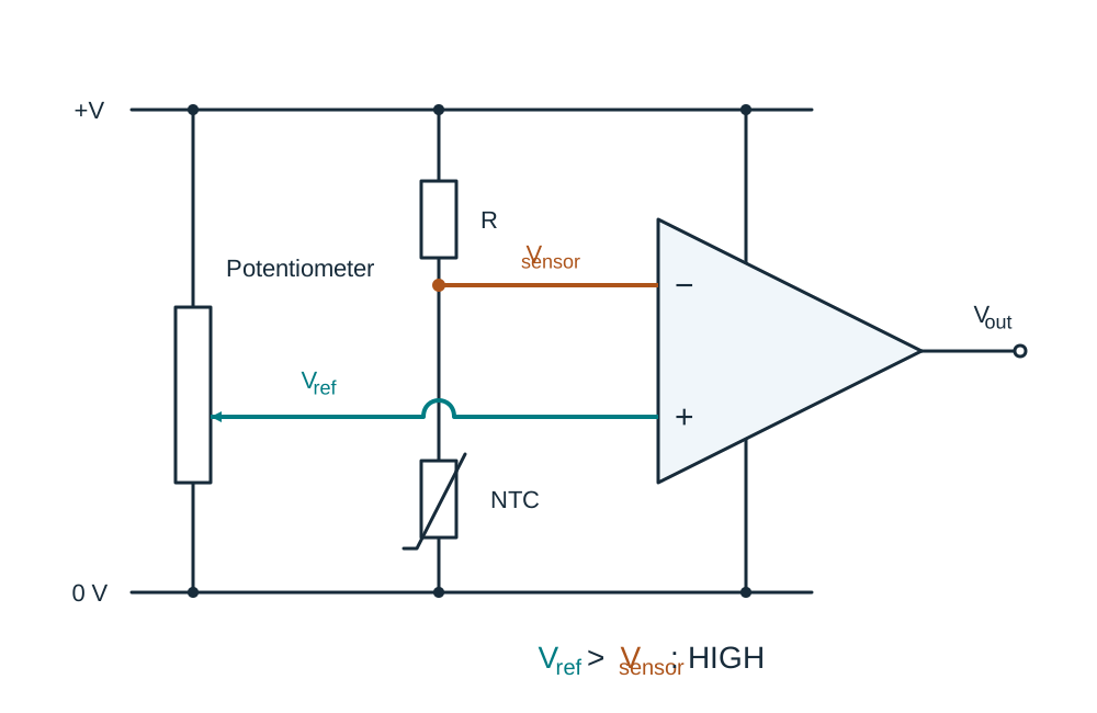
In voltage comparison mode, two separate analogue sensor voltages are compared directly (for example, two LDR potential dividers mounted on opposite sides of a solar tracking panel to identify which side is receiving more illumination).
Negative Feedback Amplifiers
Connecting a feedback resistor () from the output back to the inverting input () provides negative feedback, stabilising the circuit into a linear amplifier:
- Inverting Amplifier: The input signal connects through resistor to the inverting input, while the non-inverting input is tied to 0 V. The output signal is inverted (180° out of phase):
- Non-Inverting Amplifier: The input signal is fed directly into the non-inverting input (), keeping input and output voltages in phase:
The output voltage can never exceed the supply rails. If calculated amplification exceeds , the amplifier clips at saturation.
8. Digital Logic: Symbols, Worded Design, Truth Tables, and Families
Digital logic circuits process binary signals where logic 1 represents HIGH (supply voltage) and logic 0 represents LOW (0 V).
Drawing Logic Gate Symbols
- AND Gate: Flat back, curved semicircular nose (a 'D' shape). Output is 1 only when all inputs are 1.
- OR Gate: Curved back, pointed nose (a shield shape). Output is 1 when at least one input is 1.
- NOT Gate (Inverter): A triangle pointing to the right with a small inversion bubble on its tip. Output is the inverse of the single input ().
- NAND Gate: An AND symbol with an inversion bubble on its output. Output is 0 only when all inputs are 1.
- NOR Gate: An OR symbol with an inversion bubble on its output. Output is 1 only when all inputs are 0.
Inversion bubbles always indicate signal inversion. Inputs enter from the left; the single output exits on the right.
Truth Tables for the Five Syllabus Gates
For two inputs A and B, always list the input rows in binary counting order (00, 01, 10, 11):
| A | B | AND | OR | NAND | NOR |
|---|---|---|---|---|---|
| 0 | 0 | 0 | 0 | 1 | 1 |
| 0 | 1 | 0 | 1 | 1 | 0 |
| 1 | 0 | 0 | 1 | 1 | 0 |
| 1 | 1 | 1 | 1 | 0 | 0 |
For a NOT gate (single input A): input 0 gives output 1; input 1 gives output 0.
Method for Designing a Logic Circuit from a Worded System
Examination questions frequently ask you to draw a logic circuit from a worded specification. Follow these steps in order:
- Identify the input conditions and assign each a capital letter (e.g. A = power switch on, B = safety guard closed, C = sensor active).
- Identify the desired output condition and name it (e.g. Y = motor runs).
- Translate the worded logic: 'AND' means an AND gate; 'OR' / 'EITHER/OR' means an OR gate; 'NOT' or 'if conditions are not met' means adding a NOT gate.
- Group conditions logically: evaluate OR gates first, then route their outputs into the AND stage.
- Draw the gates from left to right, connect the signal lines, and clearly label every input line and the final output line.
For example, if an automated punch press runs (Y) only when the power is on (A) AND the operator button is pressed (B) AND EITHER guard 1 is closed (C) OR guard 2 is closed (D), the Boolean expression is . Draw an OR gate for C and D on the left, then feed its output along with inputs A and B into a 3-input AND gate driving output Y.
If failure must trigger an action (such as deploying an emergency brake or parachute when all safety checks are not met), combine the safe conditions in an AND gate, then place a NOT gate on the output so the signal becomes 1 only upon failure.
Binary Inputs and Pull-Down / Pull-Up Resistors
A logic gate input must never be left floating, as it will drift between voltage states unpredictably. Connect a push-to-make switch from +V to the gate input, and add a 10 k pull-down resistor from that same input to 0 V. When the switch is open, the resistor holds the input cleanly at 0 V (logic 0). When pressed, the input is pulled directly to +V (logic 1). Swapping their positions creates an active-low switch with a pull-up resistor.
Logic Families: TTL vs. CMOS
| Parameter | TTL (Transistor-Transistor Logic, 74xx) | CMOS (4000 / 74HC series) |
|---|---|---|
| Internal Devices | Bipolar Junction Transistors (NPN/PNP) | Field Effect Transistors (MOSFETs) |
| Supply Voltage | Strict: | Wide: typically 3 V to 15 V (up to 18 V for 4000B) |
| Power Consumption | Moderate to high continuous current draw | Near-zero static power draw; ideal for batteries |
| Unused Inputs | Float HIGH if open, but should be tied | Must never be left floating; causes erratic switching and overheating |
9. Interfacing, Buffers, Flyback Diodes, and Schmitt Triggers
A logic gate output can source or sink only a few milliamperes. Connecting a motor, solenoid, or high-current lamp directly to a gate will either prevent the device from operating or destroy the IC. A buffer or driver circuit interfaces the low-power control stage with the high-power output load.
Three Syllabus Buffer Methods
- Transistor Driver: The gate output connects via a base resistor to an NPN transistor or Darlington pair operating in saturation, switching hundreds of milliamps through a load connected in the collector circuit.
- Amplifier Buffer: An op-amp wired as a unity-gain voltage follower (output connected directly to the inverting input) provides very high input impedance and low output impedance, boosting current capacity without altering voltage.
- Paralleled Outputs: Connecting multiple identical gate outputs within the same IC in parallel increases total output drive current (fan-out). Essential Rule: All paralleled gates must be connected to the exact same input signal so their outputs are always in identical states; connecting outputs in opposing states will short-circuit the IC.
Inductive Flyback Spikes vs. Rotational Back EMF
A crucial distinction tested in Leaving Certificate examinations is the difference between back EMF and inductive flyback:
- Rotational Back EMF: A continuous opposing voltage generated internally by a spinning d.c. motor armature that naturally limits running current.
- Inductive Flyback Spikes: When current flowing through an inductor or inductive coil (such as a relay coil, motor winding, or solenoid) is suddenly switched off, the collapsing magnetic field induces a sharp, high-voltage positive spike (often exceeding 100 V). A reverse-biased flyback diode connected across the coil clamps this voltage spike, protecting the driver transistor from overvoltage breakdown.
Schmitt Triggers and Hysteresis
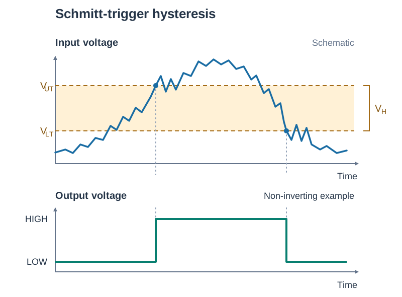
When slowly changing analogue sensor signals pass through the switching threshold of a standard logic gate, noise on the signal causes the output to oscillate or chatter rapidly between 0 and 1. A Schmitt trigger eliminates this using hysteresis, which provides two distinct switching thresholds:
- Upper Threshold (): The rising input voltage must reach this level before the output switches.
- Lower Threshold (): The falling input voltage must drop below this lower level before the output switches back.
The difference between the thresholds () is the hysteresis band. Noise fluctuations smaller than cannot trigger false state changes, resulting in clean, sharp square waves from gradual sensor transitions.
10. Sequential Counting Systems, Systematic Fault-Finding, and PCB Manufacture
A counting circuit solves a straightforward design problem: an input sensor registers an event, and we need that total displayed as a readable number.
The Five-Stage Counting System
- Input: A push switch or optical beam-break sensor generates an electrical pulse each time an item passes.
- Debouncer / Clock: Mechanical switch contacts bounce against each other upon closing, producing multiple false electrical spikes over several milliseconds. A debouncer (using an RC filter with a Schmitt trigger, or an SR bistable latch) ensures exactly one clean pulse per physical press.
- Counter IC: A 4-bit BCD (Binary Coded Decimal) decade counter (such as the 7490, CD4029, or CD4518) counts pulses from 0 to 9 in binary ( to ) across four output lines with place values 8, 4, 2, 1. Crucial Distinction: A Johnson counter (such as the CD4017) has ten discrete decoded output pins ( to ) and does not output 4-bit BCD.
- Display Driver: A dedicated IC (such as the 4511 for common-cathode displays or 7447 for common-anode displays) decodes the 4-bit BCD number into the seven active segment lines ( through ).
- Seven-Segment Display: Displays digits 0 to 9. Common-cathode displays tie all LED cathodes to 0 V and light on HIGH inputs; common-anode displays tie all anodes to +V and light on LOW inputs. Each individual segment requires a series current-limiting resistor.
Describing Circuit Operation and Suggesting Modifications
When an examination question asks you to describe how a sensor circuit operates, always describe the signal path in sequence:
- Input: State how the physical change affects sensor resistance (e.g. 'as temperature rises, thermistor resistance falls').
- Potential Divider: State what happens to the junction voltage (e.g. 'so the voltage at the transistor base rises').
- Process / Threshold: State the switching threshold (e.g. 'when base-emitter voltage reaches 0.6 V to 0.7 V, the transistor turns on').
- Logic Stage (if present): Explain how the gates process the signal.
- Output: State what happens at the output device (e.g. 'the relay energises and the alarm sounds').
To gain modification marks, state the component you would change, what you would change it to, and the resulting effect: adjust the variable resistor to alter the trip threshold; replace the single transistor with a Darlington pair for greater sensitivity; replace the transistor switch with an op-amp comparator for a sharper threshold; add a Schmitt trigger to eliminate chatter; or add a bistable latch so the alarm stays on until reset.
Systematic Fault-Finding Procedure
When troubleshooting an electronic circuit, work logically from the power supply forward:
- Visual Check: Inspect component polarity (electrolytics, diodes, LEDs, IC pin 1 orientation), cold solder joints, solder bridges, or missing wiring links.
- Power Off: Check continuity and verify there is no short circuit between +V and 0 V power rails using a multimeter on the resistance/continuity range.
- Power On: Measure supply voltages at the regulator output and at the power supply pins of every IC.
- Stage-by-Stage Voltage Checks: Measure voltage at each circuit node and compare it with the expected design value. The first node where the measured voltage deviates from the calculated value locates the fault.
- Check Logic Inputs: Verify that logic inputs are held cleanly at 0 V or +V and that no CMOS input pin has been left floating.
- Correct and Retest: Resolder or replace the faulty component, retest full circuit operation, and record the result.
Prototyping Boards, Batch Production, and PCB Manufacture
Before making a permanent board, build the circuit on a prototyping board (breadboard). Components push into connected rows of holes with no soldering required, so component values can be altered and faults traced quickly during initial testing.
Once the circuit is verified, it can proceed to printed circuit board (PCB) production:
- Prototype Production: Manufacturing a single PCB (or a few test copies) to verify track routing, component sizing, and practical operation before committing to full manufacture.
- Batch Production: Producing a quantity of identical PCBs together using the saved computer-aided design (CAD) layout. Reusing the digital file ensures every board in the batch is identical, which is how PCBs are manufactured efficiently for commercial products.
Producing a Printed Circuit Board (Photo-Etching Method)
- Design the schematic and board layout in CAD, checking track widths are wide enough for the current.
- Print the artwork onto transparent acetate to create a photographic mask.
- In subdued lighting, peel the protective backing from a photoresist-coated copper board and apply the mask.
- Expose the board under ultraviolet light in a UV exposure box for the specified duration.
- Immerse the board in chemical developer solution to wash away unhardened resist, revealing the track pattern.
- Etch the board in warm ferric chloride solution with agitation until all unprotected copper is dissolved, then wash thoroughly in clean water.
- Drill component lead holes with a 0.8 mm to 1.0 mm drill bit, clean the copper pads, and solder components in place (lowest profile components first).
- Test the finished board visually, check for rail shorts, and power up.
Safety and Environmental Care: Wear goggles, chemical-resistant gloves, and an apron when handling corrosive developer and ferric chloride. Never pour spent ferric chloride down the drain, as it contains toxic dissolved copper; store it in sealed containers for licensed disposal. CNC isolation milling provides an eco-friendly alternative that routes tracks mechanically without chemicals.
Key terms
- Indirect Measurement of Power
- Determining power by measuring voltage and current separately and calculating their product using P = V × I, rather than measuring power with a single instrument.
- Potential Divider
- A series arrangement of two resistors connected across a voltage supply that divides the voltage in direct proportion to their resistance values (V_out = V_in × [R_2 / (R_1 + R_2)]).
- Darlington Pair
- A two-transistor configuration where the emitter of the first drives the base of the second, multiplying their individual current gains (h_FE(total) = h_FE1 × h_FE2) and requiring a base-emitter voltage of approximately 1.2 V to 1.4 V to switch on.
- Rotational Back EMF
- An opposing voltage generated internally by a spinning d.c. motor armature that increases directly with rotational speed, automatically limiting running current below the stall current.
- Flyback Diode
- A diode connected in reverse bias across an inductive load (such as a relay coil or motor) to safely clamp and dissipate high-voltage inductive spikes when current is switched off.
- RC Time Constant
- The time (τ = R × C, in seconds) taken for a capacitor to charge to approximately 63% of the supply voltage through a series resistor, determining circuit timing and frequency.
- Operational Amplifier
- An integrated circuit with very high open-loop gain that amplifies the voltage difference between its non-inverting (+) and inverting (−) inputs, used for comparison, level detection, and amplification.
- Level Detection
- An op-amp comparator circuit that compares an analogue sensor voltage against a preset reference voltage, switching its output between saturation rails the instant the threshold is crossed.
- Hysteresis
- The voltage difference between the upper and lower switching thresholds in a Schmitt trigger that prevents noisy or slowly changing inputs from causing output chatter.
- Debouncer
- A signal-conditioning circuit (such as an RC filter with a Schmitt trigger or an SR bistable latch) that removes mechanical switch bounce, ensuring each switch press produces exactly one clean pulse.
- Binary Coded Decimal (BCD)
- A 4-bit digital code with place values 8, 4, 2, 1 used to represent decimal digits from 0 to 9 (0000_2 to 1001_2).
- Paralleled Outputs
- Connecting multiple identical logic gate outputs within the same IC together while feeding them the exact same input signal, increasing total current drive capacity.
Check yourself
An oscilloscope trace displays one full cycle of an a.c. square wave spanning 4 horizontal divisions with the timebase set to 5 ms/div. What is the frequency?
The period is T = 4 divisions × 5 ms/div = 20 ms = 0.02 s. Frequency is f = 1 / T = 1 / 0.02 s = 50 Hz.
Why does a stalled d.c. motor draw far more current than when running freely?
When stalled, armature speed is 0 rpm, so rotational back EMF is 0 V. Without back EMF opposing the supply voltage, current is limited solely by the very low resistance of the armature windings (I = V_supply / R_a).
Name the three methods of buffering or driving output loads specified in the syllabus.
Transistors (including Darlington pairs), operational amplifiers (voltage followers or power buffers), and paralleled outputs (joining identical gate outputs on the same IC fed from the same input).
What is the function of hysteresis in a Schmitt trigger gate?
Hysteresis provides two distinct switching thresholds (an upper threshold for rising signals and a lower threshold for falling signals). This gap prevents noisy or slowly changing inputs from causing rapid output chatter.
Why is a 10 kΩ pull-down resistor connected to a push switch at a digital logic input?
It holds the gate input cleanly at 0 V (logic 0) when the switch is open, preventing the input from floating unpredictably.
Under the 2027 Leaving Certificate examination arrangements, how many option questions must a Higher Level candidate answer in Section C?
Candidates must answer exactly one of the five option questions in Section C.